We are giving you the best knowledge on our new topic "Electronics".When you make circuits, the PCB(Printed Circuit Board) is the most significant part.You can also use Vero Boards and Dot bards,but the PCB is more professional and long lasting.All parts stick right to the board so there won't be any leaks.It is the most latest way.It takes more time than Vero boards and Dot bards to design a PCB.But after you design it successfully it is the fastest way to make circuits.
PCBs are made in several steps.

1.Designing the circuit to ready to soldier.

The designing step is the most difficult for me.Even the etching is more easier than that.The designing can be done manually drawing directly on the board and using pens and papers.But as the technology has developed we are going to use the PCB designing software EAGLE CAD.
It is also available for Linux Kernels.
So Let's get it started!

This is the Control Panel Of the EAGLE.
#1.Go to File > New > Project.We have to first start a project for the PCB.

#2.Now name it as you like.Right click on it and Choose rename.You can see your projects at the left side bar.

Now we are ready to design.
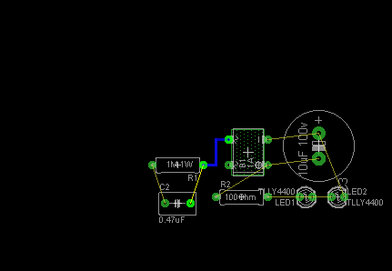
#3.Go to File menu again and get a new Schematic.

This is the Schematic drawer.You can draw any circuit here.Over thousands of components and part numbers are already in the EAGLE database

#4.Click on ADD tool to add all the components to the drawing area.It is easier to get all the Parts on to the board before connecting them with wires.
 You'll see a big window with a large number of part varieties.Choose the part you want to add and click ok.


Now draw it as much as you want.
 When you add Transistors and ICs choose the exact item.Not a dummy.Choosing the exact item will give you the right pin spacing,values, polarity connections etc.Actually the EAGLE know the uses of all the pins so you can check it with the computer for faults.When adding Capacitors,Resistors and Rectifiers the same policy applies.
Add all the parts to the drawing area.
 #5.Move your parts using the move tool.You can rotate parts with right click on the part.

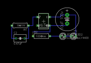
#6.Connect the pins using the wire tool and the net tool.


#7.Add junctions where they should be.


#8.Connect all the parts and draw your circuit diagram completely.Don't bother to shrink the space.Just use as much space you want and complete the circuit.

#9.Now we have to add values of the parts.This is not essential but it will be easier when you want to recognize the items in future steps.Click on the Value Tool first.Then click on the part you wish to add the value.


#10.Now we have to Generate the Board layout from this.There we make the soldier side which we want in the etching process.Click on the Generate/Switch to Board menu button.

#11.This is the board editor.Your items won't be in a good way.But don't worry we are going to fix it now.Drag all the parts in to the board first.
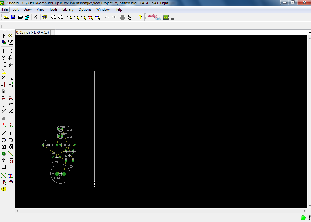

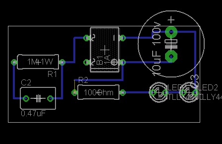
#12.Now move them and get a proper positioning where there's no overridings or shorts.

#13.If it is very difficult to get the connections right you can do it in the routing step.Click on the route tool. Draw routes like you drew wires and nets in the schematic.

#14.If you're designing a very complex circuit use the auto router.But there will be some errors in it.If you get some routing wrong , using Rip Up tool to convert them in to airways again.The yellow lines are the airways and they can be moved/edited.

Finally your board should look like this,without any errors.
Make sure your routing is the layer 16,the bottom.You can change it by using Info Tool.The red routes are the bottom ones.Click on them using the info tool and change the layer from the drop down menu.
#15.Now let's reduce the size of the board matching our circuit.Click on the move tool and drag corners of the board.

#16.Now let's draw some polygons.The polygons will,1.Save your etchant
2.Save your time when etching
3.Give the circuit a professional look
Click on the polygon tool and draw a polygon on the circuit.You'll only see the borders of the polygon first.Then click on Ratnest tool to fill up the polygon.
Add several polygons covering your whole circuit.
#17.Do not forget to save the board.!!!!!
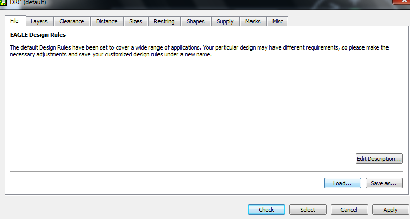
#18.Now let's give it a Design Rule Check to see the errors.Most of the errors are no critical.But there are some width and dimensional errors.


Comment your experience and share with us! Subscribe for more electronic circuits !!
PCBs are made in several steps.
1.Designing the circuit to ready to soldier.
2.Etching.
3.Drilling
4.Cleaning
Easily Applicable Graphical Layout EditorEagle Cad is very easy to use.But you must know the right controls to use.It has many advanced controls which make it easier to design.The Eagle CAD is not a freeware,but there is a Light Edition of it which has a board size limit of 6in by 4inches.You can download the Eagle CAD light version windows from this link.
It is also available for Linux Kernels.
So Let's get it started!
This is the Control Panel Of the EAGLE.
#1.Go to File > New > Project.We have to first start a project for the PCB.
#2.Now name it as you like.Right click on it and Choose rename.You can see your projects at the left side bar.
#3.Go to File menu again and get a new Schematic.
This is the Schematic drawer.You can draw any circuit here.Over thousands of components and part numbers are already in the EAGLE database
| Tool box |
#4.Click on ADD tool to add all the components to the drawing area.It is easier to get all the Parts on to the board before connecting them with wires.
Now draw it as much as you want.
Add all the parts to the drawing area.
#6.Connect the pins using the wire tool and the net tool.
#7.Add junctions where they should be.
After that step,complete your circuit design finishing like this.
#11.This is the board editor.Your items won't be in a good way.But don't worry we are going to fix it now.Drag all the parts in to the board first.
#13.If it is very difficult to get the connections right you can do it in the routing step.Click on the route tool. Draw routes like you drew wires and nets in the schematic.
#14.If you're designing a very complex circuit use the auto router.But there will be some errors in it.If you get some routing wrong , using Rip Up tool to convert them in to airways again.The yellow lines are the airways and they can be moved/edited.
Finally your board should look like this,without any errors.
Make sure your routing is the layer 16,the bottom.You can change it by using Info Tool.The red routes are the bottom ones.Click on them using the info tool and change the layer from the drop down menu.
#15.Now let's reduce the size of the board matching our circuit.Click on the move tool and drag corners of the board.
#16.Now let's draw some polygons.The polygons will,1.Save your etchant
2.Save your time when etching
3.Give the circuit a professional look
Click on the polygon tool and draw a polygon on the circuit.You'll only see the borders of the polygon first.Then click on Ratnest tool to fill up the polygon.
 |
| Polygon Tool |
 |
| Drawn borders of the polygon |
 |
| Completed Polygon |
 |
| Ratnest Tool |
Add several polygons covering your whole circuit.
#17.Do not forget to save the board.!!!!!
#18.Now let's give it a Design Rule Check to see the errors.Most of the errors are no critical.But there are some width and dimensional errors.
 |
| Design Rule Check |
Load this Design rule check to the checker.DOWNLOAD
And then Click on the Check Button.
It will show you all the errors according to our Rules and Show us where the errors have occurred.Check whether they are critical and fix them.
Now you are almost done.
#19.Make sure you have saved the board.Now we are going to print the soldier side and the component side of the PCB.Download this Cam configuration first.
#20.Now go to the project window again and open a new cam job.Choose the cam job you downloaded from me and Click open.
#21.Now Minimize that window and Go to board editor again.
#22.Click on the Cam Processor tool on the tool bar.
#23.You'll get the same cam window opened last time with the layers loaded to the right column.
Don't change any values here without knowing.Just give the File a Destination and Click Process Job.
#24.Move to the Soldier TAB and Get the soldier side saved into a file too.
Make sure the Bottom layer is selected in this window.
#25.The final step.Download this software to open your saved .PS files using Adobe Reader.
You'll get Component side and Soldier side of your PCB nicely.Print them using a Laser printer or a Photocopy machine.
Comment your experience and share with us! Subscribe for more electronic circuits !!
Comments
Post a Comment
Like our post?
Want to know more?
Please ASK!